PCB
PCB
Blog Article
HDI PCB: Revolutionizing Miniaturization in Electronics
High-Density Interconnect (HDI) PCBs are a technological marvel that have revolutionized the world of electronics by enabling the miniaturization of electronic devices while enhancing their performance. These specialized PCBs are designed with intricate interconnections and compact layouts, making them ideal for high-performance, compact electronic products. In this article, we will explore HDI PCBs, their significance, advantages, applications, and the technology behind them. Visit HDI PCB for more information.
Understanding HDI PCBs
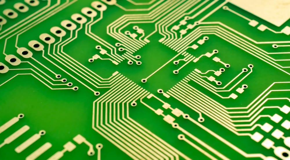
HDI PCBs are a type of printed circuit board characterized by their high-density interconnections, fine line widths and spacing, and multiple layers of circuitry. These PCBs are designed to accommodate a large number of components and connections within a small footprint, allowing for the creation of compact, high-performance electronic devices.
The key features of HDI PCBs include:
- Microvias: HDI PCBs utilize microvias, which are very small drilled holes, to establish connections between different layers of the board. Microvias are significantly smaller than traditional vias, enabling greater routing density.
- Fine Line and Spacing: HDI PCBs have finer trace widths and spacings, often requiring advanced manufacturing techniques to achieve. This allows for densely packed components and high-speed signal transmission.
- Multilayer Construction: HDI PCBs typically consist of multiple layers of copper traces and insulating material. These layers are intricately interconnected to facilitate complex electronic circuits.
Significance of HDI PCBs
HDI PCBs hold immense significance in the electronics industry for several reasons:
- Miniaturization: HDI PCBs enable the development of smaller and lighter electronic devices, making them ideal for applications where size constraints are critical, such as smartphones, tablets, and wearables.
- Enhanced Performance: The fine line widths and spacings on HDI PCBs reduce signal distortion and electromagnetic interference, resulting in improved signal integrity and overall performance.
- Increased Functionality: HDI PCBs can accommodate a higher density of components, allowing for the integration of advanced features and functionality in electronic products.
- Reduced Signal Loss: The use of microvias and advanced manufacturing techniques reduces signal loss in high-frequency applications, making HDI PCBs suitable for wireless communication devices and high-speed data transmission.
- Improved Thermal Management: HDI PCBs can incorporate advanced thermal management solutions, such as heat sinks and thermal vias, to dissipate heat effectively in compact devices.
Applications of HDI PCBs
HDI PCBs find applications in a wide range of industries and electronic products, including:
- Consumer Electronics: Smartphones, tablets, laptops, smartwatches, and other consumer devices benefit from the miniaturization and enhanced performance offered by HDI PCBs.
- Medical Devices: Medical imaging equipment, diagnostic devices, and portable health monitors utilize HDI PCBs to achieve compact form factors and high functionality.
- Automotive: Advanced driver-assistance systems (ADAS), infotainment systems, and engine control units in automobiles rely on HDI PCBs to meet space and performance requirements.
- Aerospace and Defense: HDI PCBs are used in avionics, communication systems, radar equipment, and missile guidance systems to meet the stringent demands of the aerospace and defense industries.
- Industrial Electronics: Industrial automation, robotics, and control systems leverage HDI PCBs for their high-density designs and reliable performance.
HDI PCB Manufacturing
Manufacturing HDI PCBs is a complex process that requires precision and advanced technology. Key steps in HDI PCB manufacturing include:
- Layer Stackup Design: Careful planning of the layer stackup to accommodate the required number of layers and materials while ensuring signal integrity and thermal management.
- Microvia Drilling: Precise drilling of microvias using lasers or mechanical drills to create the small holes that establish connections between layers.
- Laser Direct Imaging (LDI): LDI technology is used for precisely exposing and patterning the photoresist, allowing for fine line widths and spacings.
- Sequential Build-Up: HDI PCBs are often constructed in multiple sequential build-up stages, where layers are added and interconnected one by one.
- Quality Control: Rigorous quality control measures, including electrical testing and inspection, are applied throughout the manufacturing process to ensure that the final HDI PCB meets the specified standards and reliability requirements.
Conclusion
HDI PCBs are at the forefront of electronics miniaturization and performance enhancement. Their ability to accommodate complex designs, fine trace widths, and multiple layers of interconnections makes them indispensable in the development of cutting-edge electronic devices across various industries. As technology continues to advance, HDI PCBs will continue to drive innovation, enabling smaller, more powerful, and feature-rich electronic products.
Report this page